07 Jun 2019
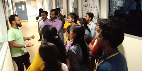
In order to promote the research ambience to our M.Tech students in the emerging technologies like MEMS & NEMS design, the School of ECE had organized an Industrial / Research Lab visit to “Centre for Nano Science and Engineering (CeNSE)”, Indian Institute of Science, Bangalore on 7th June 2019.
As per the schedule, our team reported to the PRO office - IISC, Bangalore by 2.00 p.m. After the formal procedures, they permitted to visit the CENSE research laboratories & its fabrication unit. In the CeNSE, we have been taken into two central facilities – The National Nanofabrication Centre (NNfC) and the Micro and Nano Characterization facility (MNCF).
CeNSE houses a state-of-the art National Nanofabrication Centre (NNfC) with 14000 square feet of class 100/1000 clean room. It also houses a comprehensive micro nano characterization facility (MNCF) to conduct virtually any type of electrical, optical, mechanical and material characterization. Both of these are national user facilities are accessible to outside researchers for very reasonable charges.
The Centre for Nano Science and Engineering (CeNSE) was established in 2010 to pursue interdisciplinary research across several disciplines with a focus on nanoscale systems. Current research topics include nanoelectronics, MEMS/NEMS, nanomaterials and devices, photonics, nano-biotechnology, solar cells and computational nano-engineering.
Apart from the regular faculty members at CeNSE, almost 40 faculty members from different departments at IISc are associated in the academic and research activities at the centre.
National Nanofabrication (NNfC)
• Photolithography with resolution of 1 µm for optical and 10 nm for e-beam lithography.
• Developing unit processes for chemical & physical vapour deposition, wet & dry etching.
• Fabricating complete MEMS sensors, gas sensors, GaN HEMTs, Si solar cells.
• Developing new and customized processes for MEMS/NEMS devices, microfluidic structures, and semiconductor devices for industries and other laboratories.
• Inline characterization using various metrology tools.
Micro and Nano Characterization Facility (MNCF)
• Complete electrical characterization of devices from DC to 110 MHz and at 4K to 400K temperature, using an array of probe stations and parameter analysers.
• Characterize RF devices up 70 GHz.
• Ability to measure power conversion efficiency and external quantum efficiency (EQE) of solar cells.
• Metrology of thin-films using optical profilometer; acoustic microscopy; and atomic force microscope (AFM).
• Comprehensive characterization of bulk materials and thin-films using Raman.
The students were highly delighted to experience the real time research exposure of various processes in the fabrication unit and as well as the characterization process for Micro and Nano devices. The students also gained the knowledge about MEMS fabrication from Wafer to Assembly level processing and packaging, which includes various flow of fabrication process such as Oxide growth, Thermal diffusion, Ion implantation, Deposition, Etching, Epitaxial etc.
We would like to thank our beloved Chancellor Dr. P. Shyamaraju sir for providing all facility and support to conduct such events. We also thank Vice Chancellor Dr. S.Y. Kulkarni sir, Registrar Dr. M. Dhanamjaya sir, Dean, Placement, Training, and Planning Dr. N. Ramesh sir for their constant support and encouragement.
We thank our beloved Director, School of ECE Dr. R.C. Biradar sir for his guidance and motivation to conduct all such activities.
We also thank our General Manager Col. K. Nataraj sir and Deputy GM (Admin) Mr.G.Lakshmanan sir for the logistical support in transportation. We extend thank to all the faculties and technical staffs of the School of ECE for their support.